Introduction to Electronics
Senior 6 · Physics
Introduction to Electronics
Lesson 1 of 5
25 min
Every phone, solar panel and computer depends on a strange fact. A block of very pure silicon conducts electricity so poorly that it is closer to an insulator than to a metal. Yet if one silicon atom in every ten million is replaced by a phosphorus atom, a change no chemical test would notice, its resistivity falls by a factor of about four hundred thousand (Worked example 2). The difference between copper, silicon and glass, and the reason a tiny impurity transforms silicon, both come from how electrons are allowed to be arranged in a solid. This unit starts there and builds up, device by device, to the logic gates inside a computer.
| Material | Resistivity at 20 °C / Ω m | As temperature rises, resistance… |
|---|---|---|
| copper (conductor) | rises slowly | |
| germanium, pure (semiconductor) | about 0.5 | falls steeply |
| silicon, pure (semiconductor) | about | falls steeply |
| glass (insulator) | to | stays very high |
Semiconductors are not just "medium" conductors. Their resistance falls as they warm up, the opposite of a metal, and it can be changed enormously by adding impurities or by shining light on them. Both facts are explained by energy bands.
In a single atom, electrons occupy sharp energy levels, as you saw with X-ray lines in Unit 7. When atoms are packed into a crystal, their outer orbits overlap, and by the Pauli exclusion principle each level splits into levels very close together. With about atoms in a gram, these levels form practically continuous energy bands, separated by forbidden gaps where no electron states exist.
Figure 1.1: Energy bands in the three kinds of solid (energies not to scale). Dark: filled states; light: empty states.
At room temperature the typical thermal energy is , far smaller than the gaps. Only a tiny fraction of electrons, roughly in proportion to , is thrown across. For silicon that fraction is about ; for diamond it is about , effectively zero. As the temperature rises, the fraction grows rapidly, so a semiconductor's resistance falls. In a metal, the number of free electrons hardly changes, but the vibrating ions scatter them more, so its resistance rises.
Definition
A semiconductor is a solid whose valence band is full and whose conduction band is empty at absolute zero, separated by a small band gap (roughly 0.1 eV to 3 eV), so that it conducts a little at room temperature and its conductivity rises with temperature. Examples: silicon (), germanium (0.66 eV), gallium arsenide (1.42 eV).
Worked example 1: which light can a semiconductor absorb?
A photon can lift an electron from the valence band to the conduction band only if . Find the longest wavelength that can do this in (a) silicon and (b) gallium arsenide (). (c) Explain why a silicon solar cell responds to all visible light, and why silicon looks opaque but is transparent to infrared of wavelength 1.5 µm.
Solution
(a) .
(b) .
(c) Visible light (400 nm to 700 nm) has photon energies of 1.8 eV to 3.1 eV, all above silicon's 1.12 eV, so every visible photon can create a free electron: this is how a solar cell works. A 1.5 µm photon has only , less than the gap, so it cannot be absorbed this way and passes through.
Figure 1.2: Flat models of a silicon crystal. Each double line is a covalent bond, a pair of shared electrons.
Silicon has four valence electrons, and in the crystal each atom shares one with each of its four neighbours. When a bond breaks (Figure 1.2(a)), it creates two carriers at once: a free electron in the conduction band, and a gap in the bond, called a hole. A neighbouring bonding electron can jump into the hole, so the hole moves the opposite way; it behaves exactly like a positive charge . A pure semiconductor, in which electrons and holes are made only in such pairs, is an intrinsic semiconductor, and in it the electron and hole concentrations are equal: . For silicon at 300 K, , compared with silicon atoms per cubic metre.
Both carriers drift in an electric field, the electrons against the field and the holes along it, so both currents are in the same direction. Each carrier type has a mobility , its drift speed per unit field (); the conductivity is then
For silicon, and .
Adding a carefully controlled impurity is called doping, and the result is an extrinsic semiconductor.
In band terms, donors add filled levels just below the conduction band and acceptors add empty levels just above the valence band; both gaps are tiny compared with . A doped crystal is still electrically neutral: each freed electron leaves behind a fixed positive donor ion, and each hole is balanced by a fixed negative acceptor ion.
Definition
An n-type semiconductor is one doped with donor atoms, so that its majority carriers are electrons; a p-type semiconductor is one doped with acceptor atoms, so that its majority carriers are holes. Example: silicon doped with arsenic is n-type; silicon doped with gallium is p-type.
Worked example 2: the effect of one atom in ten million
Use , and , and silicon atoms per m³. (a) Find the resistivity of pure silicon. (b) One atom in is replaced by phosphorus, and every donor is ionised. Find the new resistivity, ignoring the holes. (c) By what factor has the resistivity fallen?
Solution
(a) , so .
(b) , half a million times . , so .
(c) : the resistivity falls by a factor of nearly four hundred thousand.
Condition: this assumes that the mobilities are unchanged by doping and that all donors are ionised, both good approximations at room temperature for light doping.

An NTC (negative temperature coefficient) thermistor, made of a semiconducting metal oxide, and a coil of copper wire are placed side by side in a beaker of water with a thermometer. The water is heated slowly and stirred, and the resistance of each is read with a multimeter every 20 °C. Safety: use a hotplate or a water bath, keep the meter leads dry, and do not touch the hot beaker.
| θ / °C | 20 | 40 | 60 | 80 |
|---|---|---|---|---|
| thermistor R / kΩ | 12.5 | 5.30 | 2.49 | 1.27 |
| copper coil R / Ω | 10.0 | 10.8 | 11.6 | 12.3 |
| / | 3.411 | 3.193 | 3.002 | 2.832 |
| ln (R ÷ Ω) for the thermistor | 9.44 | 8.58 | 7.82 | 7.15 |
Illustrative readings. The copper's resistance rises by about 23%; the thermistor's falls almost tenfold. For a semiconductor, , so a graph of against (temperature in kelvin) is a straight line of gradient , from which an energy gap can be estimated.
Worked example 3: an energy from a thermistor
Use the first and last columns of the table to find the gradient of the graph of against , and hence the energy ().
Solution
Gradient .
.
Comment: 0.68 eV is the same order as the band gaps of semiconductors. A metal-oxide thermistor is not a pure, intrinsic crystal, so this is an effective "activation energy" rather than a true band gap, but the steep fall of resistance with temperature has the same cause: more carriers.

Warning
Common mistakes. (1) Saying an n-type semiconductor is negatively charged: it is neutral; "n" names the majority carrier, not the net charge. (2) Saying holes are positrons or protons: a hole is a missing electron in a bond, which moves like a positive charge. (3) Thinking doping adds electrons from outside the material: each donor atom brings its own extra electron. (4) Thinking the band gap is a physical gap in space: it is a range of energies that electrons in the crystal cannot have.
Tip
Phosphorus has five, boron has three: "five gives one away" (n-type, donor), "three needs one more" (p-type, acceptor). And for temperature: metals mind the shaking, semiconductors count the carriers.
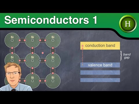
Semiconductors 1: intrinsic and extrinsic semiconductors, from Mr Smith's Physics online. Watch for how holes move and how doping with group 13 and group 15 atoms gives p-type and n-type material.
Practice
Key points
Sources and credits
The two diagrams, the experiment readings (illustrative), the worked examples and the practice exercises are written by Ganzaa. This lesson adapts CC BY-SA material and is shared under CC BY-SA 4.0.